NPGS Overview
JC Nabity Lithography Systems is the company I started as a graduate student in 1988 after it became apparent that the Nanometer Pattern Generation System (NPGS) was significantly better than any commercial SEM based lithography system available at the time. Through word of mouth recommendations alone, sales increased as I finished my Ph.D. in Physics, and at the end of 1991, I began working full time towards the sales and further refinement of NPGS. The timing was actually quite good, because while the competition had virtually a worldwide monopoly in SEM lithography, their lack of innovation, poor performance history, and incredibly high prices left many researchers wanting a high performance, low-cost system, which is exactly what NPGS provided.
Since then, word of mouth recommendations have allowed NPGS to dominate the SEM lithography market in the US, so that now researchers in almost every major research university and many government labs in the US are using NPGS. Meanwhile, the competition has significantly improved their systems (when compared to their monopoly days) and they have significantly lowered their prices (at least on their "entry-level" system), however, NPGS continues to thrive based on the unmatched performance to price ratio that it offers.
Word of mouth recommendations have also brought NPGS to researchers in Europe, Asia, Australia, and South America. (Please send e-mail if you would like the complete NPGS user list containing names, institutions, telephone/fax numbers, e-mail addresses, and microscope models or visit the User List page for a listing of the organizations using NPGS.)
By listening to the existing customers and continuously improving the system based on their suggestions, rather than just trying to generate sales through marketing and salesmanship, NPGS has earned a reputation of being the most versatile and best supported SEM based lithography system in the world.
To date, JC Nabity Lithography Systems continues to be run as a sole proprietorship with no employees, and the focus continues to be on providing a very high performance SEM based lithography system at a low cost. Time has proven that one of the advantages for customers when dealing with this "one person company" is that they always know they will be contacting the person who knows the system and who can offer complete, honest, and accurate advice on all aspects of SEM lithography. All too often, in larger companies the salespeople promise almost anything in order to get a commission based on your purchase, the support is poor because the technician's pay does not depend on your satisfaction, and there is nobody to oversee your order from start to finish, which means it rarely gets done correctly the first time. Obviously, I am not saying all other companies are like that, but if you have not had such experiences, you should consider yourself lucky.
However, a concern for some potential customers is the risk of dealing with a one person company. Questions such as "What if he retires?" or "What if he gets hit by a bus?" may come to mind. Regarding the latter, which I would categorize as an unexpected catastrophic event, the odds of such an event are actually pretty small. Considering the odds, few people would let such a question sway them from the more important questions of:
"How has the customer base for NPGS become so impressive, when NPGS is sold without any salespeople, brochures, or marketing efforts?" (Answer: The community of researchers doing SEM lithography is small enough that a high quality product with excellent support is very effectively promoted through word of mouth recommendations and "traditional" sales tactics are not required.)
and
"If the competition to NPGS has a better product and better support as their salespeople claim, how can NPGS continue to be so successful, especially when sold by a one person company?" (See previous answer.)
While researchers around the world have not considered this issue to be
significant, for anyone who might worry about retirement or catastrophic
events, please let the following reassure you. In either of these cases,
one of the following actions will take place:
- The company, including all NPGS documentation, drawings, source code, and inventory, will be sold to an established company already in a field closely related to SEM lithography. The main emphasis on company selection will be their ability to continue supporting the existing NPGS customers to the same high standards they presently enjoy. [Actually, this option is very unlikely to occur, since I don't know of any large company that offers such a high level of support, and the small companies which would qualify are successful because of their focus within their area of expertise, which does not include SEM lithography.]
- The company, including all NPGS documentation, drawings, source code, and inventory, will be sold to or jointly run with a current NPGS user who displays the necessary skills and knowledge to continue the business with the current focus on customer satisfaction. [The likely candidate for this option would be a Ph.D. graduate who feels that providing a high performance, low-cost lithography system to researchers around the world would be an interesting career opportunity, as well as a worthwhile contribution to the advancement of science.]
- All NPGS documentation, drawings, and source code will be placed in the public domain. Presently, a complete copy of this information is on a CD in a safe deposit box and instructions are in place for distribution of the information if this option ever becomes necessary.
If you are still bothered by the thought of purchasing from a one person company, I know the competition will be happy to take your money. However, if you are more interested in buying a system with a proven track record of customer satisfaction, then please keep reading the information on this site so that you can learn more about NPGS and about SEM lithography in general.
Also, at any time, please call or send e-mail regarding any questions you may have on NPGS or on SEM lithography.
Notice:
NPGS is promoted primarily by the word of mouth recommendations of the current users. Inquiries regarding NPGS (send e-mail to info@jcnabity.com) will be provided with fast, accurate, honest, and complete answers to any questions related to SEM lithography, but no follow up "sales calls" will be made, unless requested. If you think that unsolicited "sales calls" from a commission-driven salesperson asking if you are ready to buy yet are in your best interest, then please contact the competition.
Personally, I understand that the typical researcher already has too many demands on his or her time and that "sales calls" are too often just a shallow attempt by a salesperson to finalize a sale and get a commission. In contrast, my philosophy is to respect your time, which means that you will not be contacted, unless you have specifically asked for information, or have requested a follow up reminder, or significant new information can be provided regarding a previous inquiry. The ongoing success of NPGS indicates that a high percentage of researchers appreciate this approach.
As NPGS has become more popular around the world, some researchers have requested that NPGS be purchased through a local distributor. Consequently, in addition to the 'direct' purchase option, distributors for NPGS are now available in many countries.
The System:
The Nanometer Pattern Generation System (NPGS) provides a user-friendly environment for the delineation of complex structures using a commercial electron microscope. Virtually any SEM, STEM, or FIB can be used with NPGS as a powerful lithography tool for basic research and R&D applications. While no SEM lithography system can provide the speed and stitching accuracy of a dedicated beam writer, the advanced features of NPGS make it an ideal choice when e-beam lithography is needed, but the cost of a dedicated beam writer (or a modified SEM that is sold as a dedicated system) is prohibitive. Also, for many basic research applications, the capabilities of NPGS make it the preferred instrument, as shown by the fact that several customers have purchased NPGS even though they already have access to expensive beam writers.
Applications
SEM lithography can be used for the fabrication of a wide variety of devices. Research areas include: quantum structures, such as single electron transistors; optical structures, such as binary holograms and linear/circular gratings; electro-mechanical structures, such as Surface Acoustic Wave (SAW) and MEMS devices; as well as the testing of novel resists and ultra-small sensor fabrication.
Pattern sizes may range from the nanometer scale up to the maximum field of view of the microscope, which can be as large as 10 mm. However, as on any SEM lithography system, the writing resolution will decrease as the field size is increased.
NPGS is designed to be extremely flexible, yet easy to use. There are three basic steps to the pattern generation process: pattern design, parameter run file creation, and pattern writing with alignment for multilevel lithography. The fundamental aspects of each step are described below.
Pattern Design
Patterns are created using QCAD*, which is a commercial computer-aided-design program. The many powerful construction and editing features of QCAD simplify all aspects of pattern design. Many enhancements have also been added to QCAD specifically to facilitate the design of lithography patterns. All of the following drawing elements may be used in pattern design: lines of arbitrary slope, circles, circular arcs, and arbitrary filled polygons. Text, spline curves, and elliptical arcs can also be easily generated and written as series of short lines. Pattern elements that are to have different exposure parameters (such as dose, exposure point spacing, microscope beam current, microscope magnification, etc.) are designed in different drawing layers and/or different colors. This gives an almost unlimited number of exposure conditions within a single pattern. QCAD natively supports DXF and DWG formats. Patterns can also be imported from GDSII and CIF file formats.
*NPGS also still supports the versions of DesignCAD which were previously used with NPGS. DesignCAD and QCAD can be installed and used simultaneously with NPGS, if desired.
Run File Creation
Once a pattern is designed, the exposure conditions for the different drawing elements in the pattern are entered into a "Run File". This approach offers the advantage that the details of the exposure are separated from the pattern design, therefore, to vary the exposure conditions only the run file needs to be changed. Parameter entry and modification are also extremely easy. For example, a dose may be entered as an area dose (uC/cm2), a line dose (nC/cm), or a point dose (fC) and the correct point exposure time will be calculated automatically. A single run file may contain parameters for a nearly unlimited number of different patterns that will be written sequentially and each pattern may be repeated an almost unlimited number of times. In addition, advanced features include Global Stage Corrections, Pattern Arrays, X-Y-Focus, External Commands, and Fracturing of large patterns. A single run file may instruct NPGS to control the SEM in an automated mode over many hours as it aligns and writes thousands of exposures on a wafer.
Pattern Writing and Alignment
Once a run file has been created, the pattern(s) it describes may be written using the program NPGS. This program reads the run file and automatically calls the writing (PG) and alignment (AL) programs described below. NPGS can be used in a turnkey fashion with minimal user interaction, or the user can have complete control over the pattern writing - even writing patterns that were not called for in the original run file. Alternately, PG and AL are completely modular and can execute run files directly.
PG writes a pattern by simultaneously controlling the x-y scan coils and beam blanking of the microscope. The scan coils are stepped with 16-bit voltage resolution within the field of view of the microscope and the beam is blanked as needed. Patterns can be written as a series of point exposures where the beam is blanked between exposure points, or the beam can be stepped without blanking. In either case, the dwell times are controlled with better than 0.25% timing resolution at all writing speeds. To maximize throughput, the software automatically calculates the exposure points as fast as possible, independent of the actual writing speed.
Patterns may be aligned to existing alignment marks without exposing the writing area by using the alignment program AL. An alignment pattern may have several sets of windows. For example, large windows for coarse alignment followed by smaller windows for fine alignment are very useful. Each set may have up to four user defined windows anywhere on the sample. The images of the sample areas within the windows are simultaneously displayed on the PC screen. User defined overlays are also displayed superimposed on the sample images. In the Auto-Alignment mode the overlays are controlled by the computer and are individually positioned to align with the marks on the sample using a very versatile and robust cross-correlation technique, while in the semi-automatic mode the overlays are positioned manually. Once they are aligned, the program calculates a general transformation matrix that corrects for x and y magnification errors of the microscope, as well as sample rotation and offset. Signal averaging is used to optimize the image of the alignment marks for maximum alignment accuracy. This transformation matrix is subsequently used by PG when writing the pattern to give accurate registration between lithography levels.
Digital Imaging
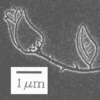
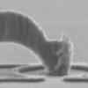
After the samples are processed, it is convenient to use the digital imaging feature of NPGS to save images of the devices. This feature has also proven to be very valuable in providing support to NPGS users around the world. For example, during the early stages when learning to do SEM lithography, developing the skill to optimization the SEM is critical when trying to obtain the finest linewidths. By using the NPGS Digital Imaging feature, users can easily e-mail JPEG images so that detailed, expert analysis of their results and suggestions on which aspects of the writing procedure they should be more careful with can be provided. Diagnostic images are also displayed on the "Sample Pictures" page on this site.
All NPGS v9 software is 32 bit and runs under 32 bit Professional versions of WinXP, Win7, and Win10, as well as 64 bit Professional versions of Win7, Win10, Win11. For a listing of the newest features added to NPGS, go to the "Upgrade History" page.