NPGS Questions & Answers
- What does NPGS cost?
- What can be done with an SEM lithography system like NPGS?
- What are the licensing benefits of NPGS?
- What is the finest linewidth that can be achieved with NPGS?
- Does the SEM need to be in a cleanroom when used for lithography?
- What brand of microscope is needed for use with NPGS?
- An SEM used for lithography can also be used for other applications. True or False?
- A new microscope is essential for lithography. True or False?
- What are my options if I install NPGS on an old SEM and then later buy a new SEM?
- Since field emission (FE) microscopes have excellent imaging resolution at low voltages, do they also produce excellent linewidths when used for lithography at low voltages?
- What is the most important factor in determining the performance of an SEM lithography system?
- As a potential new customer, why should I care that the free NPGS software updates provided for the past NPGS customers have been backwards compatible?
- QCAD must be used when doing lithography with NPGS. True or False?
- I promptly received information on NPGS after my initial inquiry, however, I have not been contacted since then for over 6 months. Why hasn't a salesperson contacted me?
- I have been talking with an SEM salesperson who recommends the competition's lithography system. Why might this happen?
- Is a Macintosh or Linux version of NPGS available?
- What is the Sherman Antitrust Act?
- Which type of writing method does NPGS utilize?
- Is a beam blanker required for SEM or STEM lithography?
- Will a microscope with a "Digital Beam Interface" work with NPGS?
- Besides the possible addition of analog XY inputs and optionally a beam blanker, the installation of NPGS does not require other internal modifications to the SEM. True or False?
- When trying to write very fine lines, what aspect of the microscope setup typically gives users the most difficulty?
- In SEM lithography, what is the most common noise problem and how can it be minimized?
- Is acoustic noise an issue for SEM lithography?
- Is the proximity effect a problem for most SEM lithography applications?
- The field size for SEM lithography is only about 100 microns, so any large patterns require a high precision stage for "stitching". True or False?
- What is the accuracy when using the NPGS Manual and Auto-Alignment?
- When "stitching" is required and alignment marks cannot be used for each field, what options are available?
- What are the sample size limitations for SEM lithography?
- What are the limitations for the writing field size?
- What are "Multiplying DACs" and why have they been used for some lithography systems, but are not used with NPGS?
- I have seen promotional material that claims multiplying DACs are faster than using a software matrix. In fact, it was claimed that the software approach is so slow it can lead to alignment errors due to stage drift. Is this true?
- I have seen promotional material that claims multiplying DACs avoid a "staircasing" effect which is possible when using a software alignment matrix. Is this true?
- I have seen promotional material regarding multiplying DACs that claims: "up to 32-bit accuracy can be achieved in alignment". Is this true?
- What resist is typically used for SEM lithography?
- What concentrations of PMMA are used?
- Where can PMMA be purchased?
- How critical is the spin speed?
- Before spinning, how is the PMMA applied to the sample?
- After spinning, how long is the sample baked?
- How can I measure the thickness of my resist?
- Does the sample have to be shielded from UV light before it is exposed and developed?
- Does exposure to the e-beam "burn away" the resist?
- What developer is used for PMMA?
- Does the temperature of the developer matter?
- Can other resists besides PMMA be used with NPGS?
- What processing is done after the resist is developed?
- What is the best approach to use when learning to do lithography?
Equipment for Lithography: (in addition to NPGS and the microscope)
- What extra equipment is needed just during the installation of NPGS?
- What equipment is needed to prepare the sample?
- What equipment is needed after the sample is exposed?
- What accessories for the SEM are required, suggested, or worth considering?
While these questions and answers apply to the typical installation, each user's application and setup is uniquely different. Consequently, it would be surprising if you did not have other questions that are not covered here. If so, please do not hesitate to have your questions answered by sending them to "info@jcnabity.com".
General:
What does NPGS cost? (go to List)
NPGS is the lowest cost high performance lithography system for SEM/STEM/FIB microscopes that is available. Please send E-mail for the NPGS pricing. If possible, include the model number and brand of the microscope to be used with NPGS, since different connections are required for different models.
What can be done with an SEM lithography system like NPGS? (go to List)
An SEM lithography system is a tool which can be used in a wide variety of applications. The basic lithography process allows patterns to be defined on a flat surface. The subsequent processing, such as metal evaporation or etching, will determine the final structure. NPGS is unique in that it provides a very flexible system which is ideally suited to the wide range of activities in basic research and R&D activities. Examples of some of the structures made with NPGS include: single electron devices, quantum chaos devices, quantum dots, tunnel junctions, one and two dimensional metal wires/films, linear/circular gratings, surface acoustic wave (SAW) devices, split gate devices, as well as "larger" structures such as micromechanical devices, waveguides, and bonding pads. Since NPGS is so versatile, it is well suited for use in almost any application that can be done with e-beam lithography. The primary exceptions are structures covering large areas which require the capabilities of a multi-million dollar beam writer. However, in some cases, the many advanced features of NPGS allow it to be used to fabricate structures that are more difficult to make on an expensive beam writer.
NPGS can also be used for lithography with a Focused Ion Beam (FIB) system. In fact, a single NPGS installation can be configured with a dual mode to control either the electron beam or the ion beam on dual FIB/SEM systems, including the Nova Nanolab and Helios models from FEI and the Crossbeam and Auriga models from Zeiss.
What are the licensing benefits of NPGS? (go to List)
The NPGS License agreement gives the original buyer full rights to use the "Microscope Installation" of the NPGS software without any time limitations, as long as it is only installed on a single PC. The PC with the "Microscope Installation" (which contains the NPGS hardware) may be moved between different microscopes (which may require different sets of cables/connections) or may be connected simultaneously to two microscopes if they are near each other (with the NPGS Output Relay Box, which allows use of one microscope or the other for lithography). Having simultaneous connections is especially useful for dual beam ion/electron microscopes.
The NPGS License agreement allows multiple "Office Installations" of the NPGS software which may be used on more than one PC within the purchaser's research group. The "Office Installation" allows full pattern and run file design/edit capabilities, but has no pattern writing capabilities, since no NPGS hardware is used. For each "Office Installation" the only cost is the purchase of one copy of the CAD program used with NPGS, which typically costs <$100 USD. Presently, four extra copies of the CAD program are included with NPGS, so multiple "Office Installations" can be done at no additional cost. Having multiple "Office Installations" of NPGS make it easy for each member of the research group to do pattern design in the convenience of his or her office.
What is the finest linewidth that can be achieved with NPGS? (go to List)
The ultimate writing resolution depends on the SEM in use, the resist, and the operator's skill at optimizing the SEM. With NPGS, features of 20 nm and less are routinely written when using a thermal FE SEM, 30 nm and less when using a 40 kV conventional SEM, and even smaller when using a high voltage STEM.
Does the SEM need to be in a cleanroom when used for lithography? (go to List)
No, a cleanroom is not necessary. In fact, most researchers doing SEM lithography do not have the SEM in a cleanroom. When a wafer is processed in a production setting, a cleanroom is essential because contamination anywhere on the wafer is likely to affect some part of the circuit. In contrast, most research applications have relatively few devices which are very small, thus the likelihood that any contamination will affect the critical areas is also very small.
Special care must be taken when an electron microscope is to be used in a cleanroom, since cleanrooms often have relatively high levels of magnetic interference, acoustic noise, and vibration.
What brand of microscope is needed for use with NPGS? (go to List)
Almost any brand or model of SEM, FIB, Dualbeam, or STEM can be used with NPGS. The basic requirement is that analog XY inputs are available. Please see "System Description" for the other connections to the microscope and "Microscope Considerations" for a list of models of microscopes used with NPGS. Even if your model is not listed, chances are excellent that it can be used with NPGS.
Customers who are planning to purchase a new SEM often ask which model is recommended for use with NPGS. The short answer is that no SEM model is ideal for lithography and every model will have some limitations. While no specific brand or model is recommended, a detailed discussion on the issues regarding each model can be provided by e-mail or telephone, once the user's budget and lithography needs are known. Also, new customers are provided with contact information for other NPGS users who are using the models under discussion. In general, a thermal FE SEM will be the best model for SEM lithography.
An SEM used for lithography can also be used for other applications. True or False? (go to List)
True. Installing NPGS on an SEM does not limit its use for any other application. Note that when another microscope accessory, such as an X-ray system, is added to the microscope, the same connection must often be shared for control of the scan coils. Typically, a switch will be used to select which accessory will have control of the port.
A new microscope is essential for lithography. True or False? (go to List)
False. A ten year old microscope of high quality can perform better for lithography than a lesser quality microscope that is new. The major improvements of new microscopes have been in the image processing capabilities, not in the basic electron optics. The point is that quality, not age, is the more important factor when deciding if a microscope should be used for lithography. Several NPGS users have installed NPGS on old microscopes, and then after funding became available for the purchase of a new SEM, they moved NPGS to the new microscope. However, while there are high quality old SEMs that can outperform some new SEMs, the best SEMs currently available for lithography are the thermal FE models sold within the last few years.
What are my options if I install NPGS on an old SEM and then later buy a new SEM? (go to List)
NPGS can easily be moved between different SEMs simply by changing the connectors between the NPGS and the SEM. A calibration parameter within NPGS will also need to be determined for the new SEM. In some cases, users have used NPGS with two microscopes by moving the NPGS PC back and forth. Or, many users have purchased NPGS for an old SEM, with the intention to move the system to a new SEM, once additional funding becomes available. Note that in some cases, an old, high performance SEM will provide better lithography results than a new SEM.
Since field emission (FE) microscopes have excellent imaging resolution at low voltages, do they also produce excellent linewidths when used for lithography at low voltages? (go to List)
High resolution for microscopy does not guarantee high resolution for lithography. Because secondary electron scattering at the surface broadens the lines, most fine lithography is done at high accelerating voltages. Research has been done with novel resists and processing techniques to allow low kV lithography, however, the finest lines are typically not as small as those written at higher voltages.
It should be noted that cold cathode FE SEMs tend to have a significant drift and noise in the beam current which can be a problem for lithography. NPGS does include a feature to help minimize the effect of beam drift, but it cannot eliminate the drift itself and cannot reduce the noise. Consequently, this feature is not very effective for cFE SEMs, but is intended for very long exposures with a LaB6 or W source, for example, when thousands of exposures are done using an automated stage.
Thermal FE sources are very stable and tend to give higher resolution lithography at high kV than a conventional SEM at the same accelerating voltage. Consequently, thermal FE SEMs are now the most commonly purchased SEM for use with NPGS.
What is the most important factor in determining the performance of an SEM lithography system? (go to List)
When using a pattern generator on the caliber of NPGS, the limitations of the SEM will determine the performance that can be obtained. In demanding applications, a second factor can be the operator skill. NPGS has been designed to be a very flexible research tool that can help the operator work around the limitations of hardware. A main objective in the design of NPGS has been to avoid introducing any unnecessary software limitations, which is in strong contrast to the approach taken by the competition.
As a potential new customer, why should I care that the free NPGS software updates provided for the past NPGS customers have been backwards compatible? (go to List)
The past history of NPGS clearly demonstrates the commitment to customer satisfaction. First, consider the typical history of users of other products: Each upgrade is provided at an additional cost. The upgrades typically replace old bugs with new bugs. The upgrades have little or no backwards compatibility, which means the user must redo their old work when it is no longer supported.
In contrast, NPGS upgrades have been designed with the customer's interest in mind. NPGS software upgrades have been provided at no cost, have been amazingly bug free (and almost immediate fixes are provided when bugs are found), and have fully supported the previous version, so that NPGS users have not had to waste time redoing previous pattern designs.
Potential new NPGS customers can feel secure knowing that the attention to customer satisfaction which has so clearly been demonstrated in the past is also underway in regards to the newest enhancements which will be released in future versions of NPGS.
QCAD must be used when doing lithography with NPGS. True or False? (go to List)
False. While QCAD is the very powerful CAD program for pattern design which is supplied with NPGS, utilities are also supplied to convert patterns from several other formats. The most common file formats that can be imported for use with NPGS are: DWG, DXF, GDSII, and CIF. NPGS also supports several versions of the older DesignCAD software.
I promptly received information on NPGS after my initial inquiry, however, I have not been contacted since then for over 6 months. Why hasn't a salesperson contacted me? (go to List)
The customers who inquire about NPGS are treated as professionals who appreciate fast, accurate, and complete information in response to their questions. It is assumed that if customers need more information, that they will then ask for more information. It is also assumed that the customer does not need to be continually contacted and pressured into making a purchase. Most researchers enjoy being able to get honest information without being subject to an ongoing sales pitch by some salesperson who may know relatively little about the actual product.
I have been talking with an SEM salesperson who recommends the competition's lithography system. Why might this happen? (go to List)
Ideally, SEM salespeople would know about the available SEM lithography systems and might even know about their track records of customer satisfaction (or dissatisfaction, as the case may be); however, that is often not the case. Since SEM lithography is a very small niche compared to the total SEM market, it is quite possible that the salesperson doesn't really know anything about SEM lithography other than the fact that the competition is active at marketing and offers commissions. Consequently, the salesperson may recommend another system based simply on the commission that they may receive for the sale.
Fortunately, since you are now reading this web site, you no longer need to rely just on the information provided by any salesperson, but can instead request the full NPGS user list. (You can also attempt to get the full user list from the competition, however, customers have reported that for some reason they seem to prefer to only give out a few carefully selected names.) Experience has shown that the best information on both SEMs and lithography systems can come from the current users, rather than from any salesperson. This is why all potential customers are encouraged to contact any number of the current NPGS users.
Is a Apple or Linux version of NPGS available? (go to List)
NPGS only runs on a PC running the Windows operating system, however, pattern files can be created on other systems and transferred to NPGS to be written.
What is the Sherman Antitrust Act? (go to List)
This is a federal law originally enacted in the US in 1890 to prevent unscrupulous behavior by companies. It is likely that other countries have similar laws. In short, one of the aspects of this law is that it is illegal for a company to try to force customers to buy one of their products through intimidation or by withholding one product unless a related product is purchased. If you ever encounter such behavior in the US, you are encouraged to report the incident to the Federal Trade Commission.
Technical:
Which type of writing method does NPGS utilize? (go to List)
NPGS uses a true vector writing mode which gives the user the maximum control over the beam. For example, the beam will move along sloped lines and tangent to arcs and circles. Also, when filling arbitrary polygons, the beam will sweep parallel to one side of the polygon as specified by the user. This approach enhances the exposure quality over systems using a simple xy raster method or one that breaks each arbitrary polygon into trapezoids with different scan directions. In addition to the vector writing mode, NPGS also provides a raster mode for writing bitmaps which can be useful for FIB milling.
Is a beam blanker required for SEM or STEM lithography? (go to List)
No, a blanker is not required, but it will make pattern writing more convenient and may improve the results for some types of patterns. It is quite easy for NPGS to move the beam fast enough between pattern elements to avoid unwanted exposure, however, there are two problems when writing without a blanker that may adversely affect some applications. The first is that the scan coils of the microscope normally require a settling time after large changes in the beam position. Normally, this is done with the beam blanked. When no blanker is available, allowing the beam to settle would cause an overexposure at the start of each pattern element. Instead, NPGS avoids the overexposure, but then the initial exposure points of each pattern element may not be properly placed after large changes in the beam, because the response time of the scan coils will be too slow to keep up the fast jump of the DACs that is used between the elements. However, it is possible to minimize this effect with NPGS using "Dump" points. The second main problem is that the beam is always hitting the sample and care must be taken to avoid unwanted exposure when the stage is moved between exposure locations. Overall, NPGS provides features to optimize the pattern writing when using a fast beam blanker, a slow shutter, or no blanker at all.
Also, the beam is on continuously as NPGS v9 steps the DACs to expose features even when there is a fast blanker present. Consequently, writing with or without a blanker does not affect the exposure, other than the two issues described above. The fast blanker is only used when jumping between different features. The jump "away" at the end of a feature is normally so fast that there negligible stray dose, while the start of the feature may have a defect depending on the length of the jump and the settling time of the scan coils as described above. In many cases, the pattern can be designed so that any initial defects are insignificant. For example, if a line starts on top of a wider lead or bonding pad, an initial defect there is usually not a problem.
For reference, an electrostatic "beam blanker" for an electron microscope typically consists of metal plates (from ~5 mm to 10 cm in length) in the microscope column with a small gap (~0.25 to ~2 mm) where the beam passes, which will deflect the beam when a voltage (from ~5v to ~400v) is applied to one plate, while the other is kept at ground potential. The beam is blanked when the voltage is applied because the deflection of the beam makes it miss the opening in a subsequent aperture or makes it hit a "knife edge" on one of the blanking plates. The beam passes with no deflection for pattern writing or during imaging when both plates are at ground potential. The repetition rate for beam blanking can range from a slow ~200 kHz to a very fast ~50 MHz, depending on the blanker. The rise/fall times for the blanking transition will typically range from <10 nsec to ~100 nsec. Some microscopes will have a ~1 MHz rate magnetic blanker or will have a slow (~5 msec) blanking capability that is produced by magnetically deflecting the beam with a gun alignment coil.
Will a microscope with a "Digital Beam Interface" work with NPGS? (go to List)
Every "Digital Beam Interface" that has been encountered has actually had analog XY inputs which are compatible with NPGS.
Besides the possible addition of analog XY inputs and optionally a beam blanker, the installation of NPGS does not require other internal modifications to the SEM. True or False? (go to List)
True. If the SEM has the analog XY inputs, no modification is required, and the use of a beam blanker is optional.
When trying to write very fine lines, what aspect of the microscope setup typically gives users the most difficulty? (go to List)
Minimizing the astigmatism is usually the most difficult part of the microscope setup. Obviously, the focus is also important, but it is usually easier to optimize than the astigmatism. Typically, the first fine patterns written by a new user will show signs of astigmatism. With practice, a user becomes able to consistently minimize the astigmatism. The NPGS User's Manual provides step by step instructions detailing one approach to writing fine features and there are diagnostic images with discussions of problems and specific instructions online.
The difficulty of minimizing the astigmatism in the beam is inversely proportional to the image quality. In other words, an SEM that gives a better image will be easier to optimize for lithography. For this reason, an FE SEM is typically the easiest to use for lithography, followed by a conventional LaB6 SEM, then an SEM with a W filament.
In SEM lithography, what is the most common noise problem and how can it be minimized? (go to List)
Line frequency interference that is picked up in the microscope is the most common problem. Typical sources are: electrical power lines, older fluorescent lights, older PC monitors (this noise is actually at the refresh rate of the monitor), ion pump power supplies, and other electrical equipment including picoammeters. Solutions are to eliminate or relocate the source of the noise, shield the SEM from the noise source, or install a magnetic field cancelling system. The Extech Model EMF510 is an inexpensive digital gauss meter for locating sources of 30 to 300 Hz magnetic fields. Also, see the Line Frequency Noise image in the Diagnostic Images on the Sample Pictures page.
Is acoustic noise an issue for SEM lithography? (go to List)
The significance of acoustic noise can easily be determined when operating an electron microscope at high magnification at a slow scan rate. When using a TEM or FE SEM, a hand clap will often cause an obvious distortion of the scan, while conventional SEMs with W or LaB6 filaments will typically be relatively insensitive to acoustic noise. By correlating the magnitude of the noise to the distortion on the screen, the significance for SEM lithography can easily be determined. For example, if a loud clap only produces a 10 nm distortion, then acoustic noise will be unlikely to affect lithography if the room is kept reasonably quite during the pattern writing. In some cases, simply talking can degrade the image, but then the simple solution is to keep quiet during image acquisition and pattern writing.
If acoustic noise is affecting a TEM or FE SEM, solutions are to cover the walls with sound absorbing panels, to place a sound absorbing curtain or box around the column, and/or to wrap the column itself with a sound absorbing material. For the last approach, materials from bubble wrap to neoprene have been successfully used.
Is the proximity effect a problem for most SEM lithography applications? (go to List)
No, for most applications the proximity effect can be easily compensated for by simple modifications to the pattern, while many applications require no changes within the pattern at all. Only a small number of research applications require an automated correction scheme. The NPGS "Sample Pictures" page shows a wide range of patterns that have been successfully written without any automated proximity correction, and typically without any proximity correction at all.
The field size for SEM lithography is only about 100 microns, so any large patterns require a high precision stage for "stitching". True or False? (go to List)
False. While pattern features less than about 0.1 microns are typically written in a field of about 100 microns, much larger field sizes can be used for larger structures. For example, it is common to use a field size of 1 mm or more when writing leads out to bonding pads and it is easy to connect these leads to features within a 100 micron field without moving the stage at all. Consequently, most electrical connections can be made by writing one small field along with a larger overlapping field which avoids the need for any "stitching" of small adjacent fields. When the "stitching" of fields is required, the advanced Auto-Alignment feature of NPGS can often be used to get very accurate alignment of fields when using a low precision automated stage or even a manual stage. For many applications, this versatility of NPGS can save $150,000 USD or more by eliminated the need for an expensive high precision stage.
What is the accuracy when using the NPGS Manual and Auto-Alignment? (go to List)
When the NPGS Alignment feature is used to register to alignment marks, the accuracy is typically from 1:1000 to 1:3000 of the field of view and results to 1:5000 have been reported. For example with a ~90 um field, the alignment accuracy will typically be from ~90 nm to ~30 nm. Note that the accuracy is independent of the stage (assuming the initial positioning is good enough that the registration marks can be seen within the alignment windows), which is why accurate alignment can be achieved even with a manual stage.
When "stitching" is required and alignment marks cannot be used for each field, what options are available? (go to List)
There are options for stages with higher resolution than a standard automated SEM stage, as listed under the "Microscope Accessories & Services" section of the "Other Resources" page of this site.
What are the sample size limitations for SEM lithography? (go to List)
There are three basic questions regarding sample size.
First, will the sample fit into the SEM? - Almost all SEMs will hold a 2" or 3" wafer and some can accommodate an 8" wafer. (Note that the maximum sample size for an STEM will typically be only about 10 mm by 3 mm.)
Secondly, what is the stage travel of the SEM? - Most SEMs have 2" of stage travel, some have 4" of travel, and a few have up to 8" of travel. In some SEM models with limited travel, it may be possible to put in a stage with longer travel, if there is enough room in the sample chamber.
Thirdly, what is the practical limit of how many exposure fields can be written with an SEM? - The total number of fields is limited by the writing time of the patterns and perhaps by the stage travel time as well. Individual patterns may take from seconds to hours to write, depending on the size of the writing field, the beam current used, and the pattern density. One NPGS user has been writing thousands of fields with total writing times of ~8 hours, however, the specifics of each application need to be considered before an accurate evaluation can be offered.
A related question is how large of an area can be covered using SEM lithography? For ~0.25 um features, an SEM can typically write over about a 500 micron square field. Using this writing field size, it would take ~2,500 fields to cover a 1 inch square area and the total time would be ~7 hours if each field could be completed in ~10 seconds (including stage movement, stage settling, optional automated pattern alignment, and pattern writing). When writing over long periods, the stability of the SEM can be a concern.
What are the limitations for the writing field size? (go to List)
The maximum writing field size for a single exposure is set by the SEM's magnification. The largest writing fields will be from 5 to 10 mm square, depending on kV and working distance. However, the writing resolution depends on the field size, so fine features must be written with smaller fields. For most SEMs, the finest features (<50 nm) are written with a field size of ~100x00 um2. Features on the order of ~200 nm can written with a field size of ~400x400 um2, while larger features can be written at the largest possible field size, i.e., at the lowest magnification of the SEM.
What are "Multiplying DACs" and why have they been used for some lithography systems, but are not used with NPGS? (go to List)
Multiplying DACs allow a reference voltage to be scaled by a value determined by a digital input. Consequently, if the output of another DAC is used to set the reference voltage, the multiplying DAC can scale the final output as follows: X' = A*X, where X' is the final output voltage, X is the voltage of the first (non-multiplying) DAC, and A is the scaling value set for the multiplying DAC. If four multiplying DACs are used and the intermediate results are properly summed, a 2x2 transformation matrix for pattern rotation can be generated by the hardware.
NPGS does not use multiplying DACs in this fashion, because this approach is not necessary. Instead, NPGS does the matrix calculation in software using 32 bit arithmetic and then outputs the final XY values through a single set of 16-bit DACs. Consequently, the alignment matrix elements can be expressed in software to a higher resolution than the hardware approach, and the matrix does not have any limitations in possible values as in the case of the multiplying DACs. However, in practice, it is unlikely that any difference will be seen between the two approaches, assuming that the hardware used in the multiplying approach has been properly designed to minimize the added noise of the extra components.
*I have seen promotional material that claims multiplying DACs are faster than using a software matrix. In fact, it was claimed that the software approach is so slow it can lead to alignment errors due to stage drift. Is this true? (go to List)
No. Back in the days of PC's with 80386 processors, the software approach was obviously slowed by the extra calculations, however, the additional time was typically a matter of extra "seconds" for each million exposure points. If the stage drift is enough to make this extra time a problem, then it would be impossible to do any reasonable alignment at all. With the speed of a new PC, the calculation speed is so fast the claim is even more inappropriate. In a test some time ago with a 300 MHz Pentium II, a pattern with 10 million points showed less than a 0.5 second delay when aligned in software using an arbitrary 2x2 transformation matrix plus XY offset. With a modern PC, the extra calculation time is completely negligible.
*I have seen promotional material that claims multiplying DACs avoid a "staircasing" effect which is possible when using a software alignment matrix. Is this true? (go to List)
No. As background information, the "staircasing" effect is when the resolution of the exposure point placement is coarse enough that sloped edges will have steps from point to point, similar to a staircase. Staircasing has never been reported with NPGS, because the full 16-bit resolution of the DACs is always used. Even when a low magnification is used such that the 16th bit of the DACs represents a relatively large step on the sample (for example, at 100x a typical 16th bit will be ~14nm), the limitations of the SEM will prevent such small features from being written anyway. Consequently, the use of an alignment matrix applied through software does not lead to "staircasing" with a well designed system like NPGS.
Ironically, "staircasing" was a problem with the older systems sold by the competition, because they previously used a very limited writing scheme which effectively threw away the higher precision bits of the DACs when writing many patterns. However, since then they have improved their system by copying the approach pioneered by NPGS.
*I have seen promotional material regarding multiplying DACs that claims: "up to 32-bit accuracy can be achieved in alignment". Is this true? (go to List)
No. An alignment accuracy of 1:1000 (~10 bit) means the error will be 100 nm for a 100 micron field. NPGS users have reported that they have always achieved the alignment accuracy needed for their applications (which is what is important), and upon inspection the numbers show the accuracies have been up to 1:5000. Now, an alignment of accuracy of 32 bits would mean 1 : 4.3 billion, or an accuracy of 1 Angstrom in a field of 43 centimeters, which is clearly unrealistic.
What the claim was probably trying to imply was that the outputs from the 16-bit DACs which are stepped from point to point are then run through additional 16-bit multiplying DACs. Simple math gives 16+16=32 bit accuracy. However, this simplistic evaluation is invalid. The noise of the all of the DACs will be added in some fashion (the exact expression would depend on the details of the circuit), such that is it very unlikely the final output could be any better than 16-bit resolution. Also, even if a higher resolution output were achieved, the internal noise of the SEM could make it unnoticeable. The bottom line is that any calculated measure of alignment accuracy should be ignored and only real results from unbiased users should be considered.
*If you have seen other misleading or obviously false claims from competing systems, please send them to "info@jcnabity.com" so that accurate information can be presented here.
What resist is typically used for SEM lithography? (go to List)
PMMA, poly(methyl-methacrylate), with a molecular weight of 950,000 is the most common resist used for fine lithography because of its high resolution. PMMA with lower molecular weight is typically used for the bottom of bilayers, where the top layer is the 950k PMMA. Other positive and negative resists are available, but they typically do not have the high resolution of 950k PMMA. For a discussion of resists for e-beam lithography, please see the Chapter 2 of the SPIE Handbook of Microlithography. The handbook can be ordered through Amazon at Handbook of Microlithography, Micromachining, and Microfabrication : Microlithography. Additional information on e-beam resist processing is available at CNF.
What concentrations of PMMA are used? (go to List)
The concentration of the PMMA in solution will affect the thickness after spinning onto the substrate. I have used 3% by weight in chlorobenzene, which gives about 150-200 nm when spun at 4000 rpm, and 6% which gives about 600 nm when spun at 4000 rpm. The resist supplier MicroChem has charts showing thickness vs. spin speed for various concentrations in the two most common solvents of chlorobenzene and anisole. (Note that anisole is a less hazardous solvent that is often used with PMMA.) You may use the link in the next item to get to the the MicroChem web site and request additional information from them.
When multiple concentrations are desired for different applications, a cost effective approach is to purchase a relatively high concentration of PMMA and also the solvent. Subsequently, portions of the high concentration resist can be diluted to other lower concentrations, as needed.
Where can PMMA be purchased? (go to List)
The "Other Resources" page has several suppliers of resist for e-beam lithography. For small quantities of premixed PMMA, you may want to start by contacting MicroChem, Inc.
How critical is the spin speed? (go to List)
A faster spin speed can result in a thinner resist layer, however, too fast can cause variations in the thickness. Too slow of a spin speed can also cause problems. Since even small variations in the thickness will be visible, you can try different spin speeds and simply wash off the resist with acetone when the results are not acceptable. For full wafers, a "pre-spin" or acceleration time can be used to cause the resist to spread evenly over the wafer before the final spin speed will produce the final thickness. For example, I have used a pre-spin of 500 rpm for 3 seconds or an acceleration time of 1 second on different spin coaters.
Before spinning, how is the PMMA applied to the sample? (go to List)
I suggest using disposable glass pipets for dispensing the PMMA onto the sample while it is stationary. This allows the resist to be taken from the center of the container which avoids getting any dried particles that can result when it is poured out and it avoids contamination since a new pipet is used each time. Also, before the PMMA is applied, it is common to give a final cleaning using acetone and alcohol. For this you should have the sample spinning when you begin squirting it with acetone. Then start squirting it with the alcohol before you stop spraying the acetone. After stopping the alcohol, let the sample spin until it is dry.
After spinning, how long is the sample baked? (go to List)
One method for PMMA is to bake the sample at 160C for 2 hours or more in an oven, while another method is to put the sample on a hot plate at 180C for 15 seconds to a minute. Personally, I prefer to use an oven, since the internal temperature is controlled much more precisely than the surface of the sample on a hot plate, however, many different baking recipes are in use with good results.
How can I measure the thickness of my resist? (go to List)
If you don't have access to specialized equipment for precise height measurements, the easiest approach is to: a) Spin resist on a test sample and bake it as usual; b) Coat the sample with a thin layer of gold; c) Cleave the sample and mount it in the SEM so that the cleaved edge can be viewed. While SEM distance measurements must be compared to a known standard before they can be trusted, for thickness measurements of resist, the typical accuracy of the SEM size marker should be good enough.
Does the sample have to be shielded from UV light before it is exposed and developed? (go to List)
The PMMA has a low sensitivity to UV light. Consequently, short exposure to normal room lighting during handling does not do any significant exposure. When the sample is not being handled, simply wrapping its container in aluminum foil is an easy way to stop any exposure to light. I have seen fine lithography done on PMMA coated samples that have been stored this way for over a year before the pattern was exposed.
Does exposure to the e-beam "burn away" the resist? (go to List)
No, when using a positive resist like PMMA, the exposure will break many of the bonds of the large PMMA molecular chains, and the smaller chains will be more soluble in the developer than the unbroken (unexposed) chains. When using a negative resist, the resist will start with smaller molecular chains and the beam will cause "cross-linking" to form a less soluble material. Consequently, for a negative resist, the unexposed areas will be removed during development, while a positive resist will have the exposed areas removed during development. In neither case is the resist removed during the exposure to the beam. (Actually, if an extremely high beam current is used, organic materials such as PMMA may be removed from the specimen, however, that is rarely an issue for SEM lithography.)
What developer is used for PMMA? (go to List)
Commercial developers are available, however, a common approach is to use a solution of 3:1 IPA:MIBK [or more precisely, 3 parts isopropyl alcohol to 1 part methyl isobutyl ketone, or as the bottles may be labeled: 3 parts (2 propanol) to 1 part (2-pentanone,4-methyl)]. With this concentration, typical development times are about 1 minute. An alternate recipe is to use a 1:1 or 1:2 solution where the development time may be 30 seconds or even less. Also, pure IPA can be used to develop PMMA.
Does the temperature of the developer matter? (go to List)
Yes. The most important aspect is to use a constant temperature for the developer. The most common procedure is to use room temperature or a bath heated to slightly above room temperature. Alternately, the developer may be cooled to well below room temperature, for example -15C, which may improve the resolution. In some cases, sonication may be used during the development.
Can other resists besides PMMA be used with NPGS? (go to List)
Certainly. Any resist that is sensitive to the e-beam (or ion beam when a FIB is used with NPGS) can be exposed. The information presented on the NPGS web site and in the NPGS manual describes the typical processing with PMMA, however, other resists are also available and many techniques for multilayer resist processing are commonly used by researchers using NPGS.
One interesting class of negative resist is HSQ (Hydrogen Silsesquioxane) which is available in a variety of "FOx-N" formulations (where N is an integer) and XR-1541 resists from Dow Corning.
What processing is done after the resist is developed? (go to List)
After development, many things can be done with the sample. The typical process is to evaporate a metal and to do "lift-off". For lift-off, you put the sample in acetone which will dissolve the PMMA causing most of the metal to float away. If everything works, only the metal deposited onto the substrate in the patterned areas will remain. Variations on this approach range from boiling the sample in the acetone (not recommended for safety reasons), to using an ultrasonic cleaner, to simply letting it soak at room temperature.
In some applications, the sample will be etched after development to transfer the pattern into the substrate. The etch may be done using a reactive ion etcher or just a wet chemical etch. Also, the resist itself may be used as the etch mask or a more resistant material may be necessary.
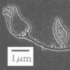
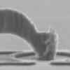
Another process is to electroplate a metal into the patterned areas. Pictures of patterned resist before and the final deposited metal are shown on the "Sample Pictures" page as "Electroplated SAW Device".
What is the best approach to use when learning to do lithography? (go to List)
When learning to do lithography, it is best to sputter AuPd (or some other metal with a small grain structure) onto the sample after development and to look at the results in the SEM without doing any lift-off. This approach provides the most information on the quality of the pattern writing. For example, if a pattern is somewhat underexposed, it will still be visible after being coated with a metal, but if lift-off is attempted, all traces of the pattern will most likely be removed. Consequently, it is better to wait to attempt lift-off until after the pattern writing is mastered.
Also, the sputtering of the metal will be more likely to coat the edges of the developed areas which will make lift-off difficult, however, it will improve viewing since the sample will be less likely to charge. For example, if a hollow ring is exposed and good undercutting is achieved, the center of the ring will quickly charge if the sample is coating by evaporation.
It is also a good idea to view the sample in an optical microscope after the development step. While fine features cannot be resolved, it is possible to check if the patterns are there or not, which can save significant time when compared to searching with the SEM.
A step-by-step procedure for doing lithography is given in the NPGS manual. Other information is also listed in the summaries for the Diagnostic Images on the Sample Pictures page on this site.
(in addition to NPGS and the microscope)
To download a PDF file containing a checklist of the required and recommended equipment for the NPGS on-site Installation & Training, click: Training_Checklist.pdf.
What extra equipment is needed just during the installation of NPGS? (go to List)
Normally, no additional equipment is needed during the installation of NPGS. However, in a few cases, an oscilloscope may be useful to check the performance of the beam blanker and/or the output voltage of the microscope image signal. Please see the "Microscope Considerations" page for a list of tests for checking the performance of a blanker. Note that even when a factory installed blanker is purchased with a microscope, the blanker may never be tested by the SEM technician during the commissioning of the microscope, unless specifically requested by the customer, and even then, the technician will rarely have any documented testing procedure.
What equipment is needed to prepare the sample? (go to List)
a) Resist Spinner - Suppliers of tabletop spin coaters are given on the "Other Resources" page. Used equipment dealers may also have commercial spinners, but they may still cost as much or more than new a tabletop model. (PMMA coated samples will be supplied during on-site installation & training.)
b) Fume Hood - It is best to do all of the spinning and sample development in a fume hood.
c) Oven - When using PMMA, one recipe is to bake at 160C for >2 hours after it is coated, while others use times as short as 15 seconds on a hot plate at a higher temperature.
What equipment is needed after the sample is exposed? (go to List)
a) The actual development for PMMA is very simple and only requires a fume hood, a timer, two small beakers*, and compressed N2 to blow off the sample, in addition to the MIBK and IPA as described above (*optionally, a third beaker may be used if a final DI water rinse is included). Self-closing tweezers are also highly recommended when working with small samples. Note that for most research applications, a clean room is not needed.
b) Optical microscope - It is very useful to inspect the sample after development using an optical microscope. Even though the lines in the patterns may be much narrower than the wavelength of visible light, you will still be able to see if the patterns came out or not. It may take some practice to spot the small patterns in the optical scope, but it can be even more difficult to find them with the SEM.
c) Sputtering System - A sputtering system is very useful when first learning to do lithography. When learning, it is best to coat the sample with AuPd (or any other metal with a small grain structure) after it is developed. The sample can then be observed in the SEM without doing any lift-off.
d) Evaporator - Many types of devices are made by evaporating one or more metals onto the patterned resist and to follow with a "lift-off" step to remove the excess metal. When doing lift-off, the evaporated metal should be only about 1/3 of the thickness of the resist layer (possibly thicker when a bilayer resist is used). For PMMA, the lift-off process itself can be as simple as soaking the sample in acetone until the metal film has floated away. More aggressive techniques include spraying the acetone onto the sample or using an ultrasonic cleaner. Note that a single layer of PMMA is often sufficient for many lift-off applications.
e) Etcher - Many types of etching systems can be used to transfer the pattern written in the resist to the substrate below.
What accessories for the SEM are required, suggested, or worth considering? (go to List)
a) XY Input - [Required] On some microscopes the external XY inputs are provided as an option at additional cost. The required connections may be part of an x-ray interface option. If the microscope also has an x-ray system or a digital imaging system that uses the XY inputs, then a manual switch or relay box will be needed to allow both NPGS and the imaging system to have access to the scan control input connector.
b) Picoammeter & Faraday Cup - [Required] A picoammeter is essential for measuring the beam current before each session of pattern writing. A Faraday cup is used to collect the beam for measuring. A Faraday cup can easily be made by drilling a small hole (~2 mm dia.) a few millimeters deep into the sample holder. After coating the inside of the hole with carbon paint, it can be covered by an aperture with a diameter less than a few hundred microns. (Apertures for this purpose are included with NPGS.) In some cases, people have used aluminum foil with a pin hole in place of a manufactured aperture. The picoammeter is then attached to the specimen current connection on the microscope.
c) Image Signal Output - [Required] This is normally a standard feature of most microscopes. It provides a voltage signal that is proportional to the secondary image intensity and is used by NPGS for the system calibration and for the manual and auto-alignment modes.
d) Beam Blanker - [Optional, but recommended] A beam blanker is not required for lithography, but having one is generally recommended. Many researchers with older microscopes are doing good lithography with no blanker, while researchers who are purchasing new microscopes usually make it a point to include a blanker. Note that some SEMs are sold with a slow beam shutter that has a response time of several milliseconds. These can be used with NPGS, but they do not offer the advantages of a fast (~1 MHz or better) beam blanker. Also, some new electrostatic blankers are sold without the low-noise electronics to energize the plates. NPGS can provide a digital signal to indicate when the beam should be on or off, however, this signal is not designed to directly energize the plates in the microscope column. Depending on the voltage required on the blanker plates, blanker electronics are available that are fast and low-noise.
e) Automated Stage - [Optional] An automated stage can be quite useful for lithography, especially when the number of exposures gets large enough that it is a nuisance to be moving the stage by hand. All but the lowest cost new microscopes will include an automated stage as a standard feature. Many older models can be retrofitted with a relatively inexpensive (~$15k USD) stage controller that provides joystick and external control for the stage positioning. Software drivers for many common stages are provided at no charge with NPGS and custom drivers can be provided on special request or they can be written by the user. Stages that use piezoelectric positioning and/or laser interferometers to provide higher resolution can also be retrofit to some SEM models, but these stages typically have limited travel and/or limited control (i.e., no rotation, tilt, and/or z positioning), so most lithography is done with the standard SEM stage.
f) Digital Interface - [Optional] Most of the newer SEMs have a digital interface (typically RS232 or Ethernet) that is either standard or available as an option. NPGS can be interfaced to such microscopes so that it can automatically set the microscope parameters such as magnification and coarse beam current or spot size. Software drivers for many common microscope interfaces are provided at no charge with NPGS and custom drivers can be provided on special request or they can be written by the user.
g) Digital Imaging Systems - [Optional] Any newer SEM will have a digital imaging system. For microscopes without a digital imaging system, NPGS includes a digital image acquisition feature that can save images in many common graphics formats. While digital images are not needed for lithography, they can be very useful for normal imaging applications. One use for them in lithography is that they make it easy to send pictures of exposed patterns by e-mail for evaluation. This allows problems with the writing, which are typically caused by SEM/blanker problems, electrical/magnetic noise, or operator error, to be more easily evaluated.
When a 3rd party digital imaging system is present on the microscope, it is necessary to check if the imaging system takes active control of the beam position. Since NPGS also takes control of the beam position, a manual switch or relay box will be needed to allow both NPGS and the imaging system to have access to the scan control input connector.
h) LaB6- [Optional] The main benefits from having a LaB6 source are that the image has a higher signal to noise, which makes it easier to consistently optimize the microscope before pattern writing, and the longer lifetime of the tip vs. a tungsten filament. When the microscope is properly optimized with a LaB6 or W filament, it has not been seen that there is a significant difference in the actual writing.
i) Field Emission - [Thermal models are recommended, if you can afford one!] Cold cathode FE SEMs tend to have a significant drift in the beam current which can be a significant nuisance for lithography, although some of the newest cFE models have much less drift/noise than the older models. Thermal FE SEMs have a much more stable beam and are preferable for lithography. Note that it is not an option to change between a W or LaB6 tip and a FE source.
j) Scan Rotation - [Optional, but recommended] This allows the writing (scanning) axes to be rotated about the center of the field of view. This is a very useful option to have for lithography.
k) X-Ray Analysis System - [Not used for lithography] Many SEMs are used for x-ray analysis. The main conflict between NPGS and an x-ray system is the access needed for the scan control input of the microscope. If the x-ray system takes active control of the beam position, a manual switch or relay box will be needed to allow both NPGS and the x-ray system to have access to the scan control input connector. Also, an x-ray system may communicate with the microscope through the same digital interface used by NPGS. Different solutions exist for sharing the digital interface depending on the microscope model.
l) Other options - New SEMs may have many other options. If you have questions about any of these, please send e-mail to the address given below.