 Thermal
FE Image:
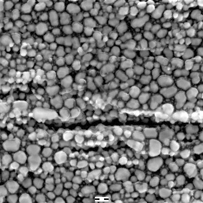
Thermal
FE Image:
These images show pictures of a gold resolution standard after the SEM has been reasonably well optimized. The marker in both images is 100 nm. (This image was acquired with the NPGS Digital Imaging Feature.)
The top image was taken on a field emission SEM at 30 kV, which will give better clarity than a microscope with a tungsten or a LaB6 source. However, the key point for SEM lithography is to minimize the astigmatism, which can be done with any filament type, even though the ultimate imaging resolution may vary widely.
Gold resolution standards like this can be purchased from microscope supply companies which are listed on the "Other Resources" page. Note that some gold resolution standards may have much larger gold islands, however, the small islands as shown here are best for optimizing the SEM at high magnifications.
To see an example of a pattern which has been exposed after an almost ideal SEM optimization, click "Wheel #1".
 LaB6
Image:
LaB6
Image:
This image was taken at 30 kV with a beam current of 20 pA at 7 mm working distance on an SEM with a LaB6 filament. As expected, the image resolution is not as good as the image above, which was taken on a field emission SEM. Similarly, an image taken on an SEM with a tungsten filament will typically not have the image quality shown here.
For more information, see the general SEM Optimization Guide and the SEM Lithography Setup Guide.