
NPGS: Solutions to Problems
This list includes problems that can apply to any microscope used for lithography.
For specific solutions regarding NPGS issues, including the QCAD and/or DesignCAD software, please see the manual accessible through NPGS.
If you have a problem that is not discussed here or elsewhere in the NPGS manual, please call or send e-mail with a detailed description of the problem so that a solution can be found.
Please select topics from the following list or scroll down to see all of
the information:
| Pattern Exposures |
Beam Blanker
|
Pattern Exposures
· When I write fine lines, the exposure varies for lines at different angles.
· When I expose single dots, the dots are elongated rather than round.
· When I write fine circles, the line width varies between wide and thin every 90 degrees.
All of these problems are almost always caused by astigmatism in the beam. The astigmatism either is present when the samples are being viewed or was present when they were being written. If the pattern contains circles with radial spokes, i.e., a "wheel" (see Sample0.dc2 in NPGS), the exposure is especially revealing. When the linewidth changes between wide and thin every 90 degrees it is a sure sign that there is or was astigmatism in the beam. In some cases, the astigmatism is in the beam during the imaging, while the beam used for the pattern writing may have been fine. The test for this is to sweep back-and-forth in focus while imaging to see if the direction of the astigmatism changes. If the direction changes, then the astigmatism is in the beam used for imaging. If the astigmatism direction does not change, it was in the beam during the lithography. When first learning to do lithography, the case where both the writing beam and the imaging beam were not optimized well may also be encountered.
In fact, a circle or ideally a "wheel" exposed by a single pass of the beam should be incorporated into every test pattern in order to detect astigmatism. Unfortunately, the results are not known until the sample is processed, but it still provides an excellent gauge of how well the microscope was set up for the pattern writing. With a little practice, most people can consistently set up the microscope to minimize the astigmatism well enough for very fine lithography.
For images showing the results of astigmatism during the exposure, please visit the "Guide to Common SEM Lithography Exposure Problems" on the "Sample Pictures" page.
Pattern Aspect Ratio (go to Top)
· When I write circles they do no turn out round and squares turn out as rectangles.
This may mean that the aspect ratio for the pattern writing system needs to be adjusted. For NPGS, see the NPGS Manual and/or the NPGS Installation Guide for complete details. For NPGS, this is usually a one-time procedure and should be done during the initial installation.
If patterns only occasionally have a distorted aspect ratio, the cause may be that a "tilt correction" mode of the SEM was enabled during the pattern writing. For lithography, any tilt correction mode of the SEM should be disabled. For distortions on the order of a few percent, it is quite possible that the microscope's aspect ratio for the XY inputs changes as the magnification has changed, but errors on this level are typically within spec for an SEM. Another possibility is that the "scan rotation" option of many microscopes may introduce aspect ratio errors on the order of a few percent.
Pattern Distortion from Charging (go to Top)
· When I write a large pattern on a low conductivity substrate some parts of the pattern turn out distorted while other parts are fine.
The sample is probably charging during the pattern writing enough to deflect the beam in some areas. Please see the "Charging (during writing)" diagnostic image on the "Sample Pictures" page of the NPGS web site for more information.
One solution is to evaporate ~100 Angstroms of aluminum on top of the resist before writing and etch it off in NaOH or KOH after the writing and before developing. One recipe is to use several pellets of NaOH in ~100 ml of DI water and etch for about 30 seconds. (You can coat some test samples and try various concentrations and times to optimize the process, if necessary.) Note that NaOH may permeate the PMMA and chemically interact with some substrates. Other metals such as Au, AuPd, or Cr can also be used with the appropriate etch after exposure. Also, conductive polymers may be used.
Another solution when an 'Environmental' or 'Variable Pressure' SEM is being used is to introduce a low pressure of gas (typically water vapor, N2, Ar, or He) to avoid charging effects during lithography.
Pattern Noise from Environment (go to Top)
· My patterns have a significant noise problem (either line frequency or even a square wave at some other frequency) even though the PC chassis is grounded directly to the microscope chassis.
The most common source of noise is magnetic pickup at line frequency. Please see the "Line Frequency Noise" diagnostic image on the "Sample Pictures" page of the NPGS web site for more information.
Three possible solutions are:
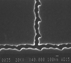
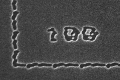
The images below show severe cases of 60 Hz pickup from a nearby power bus. Mu-metal shielding around the SEM chamber significantly reduced the noise. The lines were written with a single pass of the beam and the line widths in both images are about 150 nm.

|

|
In general, the appearance of line frequency noise pickup may range from the "choppy" interference shown here to almost perfectly smooth sinusoidal oscillations. The identifying characteristic is that the period will correspond to the local line frequency. To determine the frequency of the interference from a micrograph:
Also, some SEMs will have internal pickup on the xy scan lines depending on the SEM scan mode and magnification that is used for the pattern writing. In theory, the SEM scan mode should have no effect on the pattern writing because the microscope is under external control, but in some cases it does matter. For example, on some older model JEOL SEMs, interference from the internal scan generator may be superimposed on the pattern if the microscope is in the SR (Super Rapid) or TV mode during writing, while a Slow Scan mode will appear fine.
The magnification used for pattern writing can also affect the interference that is seen in the patterns. SEMs have different circuits that are used for different ranges of magnification and the low end of each range will have the best signal to noise, and consequently, the least sensitivity to internal interference from the microscope. Typically, when the SEM changes from one magnification range to another, an audible click may be heard and/or a glitch may be seen on the SEM image. For more information, see "Pattern Noise from SEM" below and "System Installation: Check List" in the NPGS User's Manual.
Pattern Noise from SEM (go to Top)
· My patterns were writing perfectly at 1000x, but now have a noise problem at 900x.
· My patterns were writing perfectly at 100x, but now have a noise problem at 90x.
The typical design of the scan coil amplifier circuits in SEMs is such that the signal to noise for pattern writing will vary as the SEM magnification is changed. For example, in older JEOL microscopes (models 6400 and earlier), patterns over a field of view of 900 micrometers square may be conveniently written at a magnification of 100x, however, slightly larger patterns should not be written at 90x or the noise level will be about ten times worse. Typically, for older JEOL microscopes, the best signal to noise will be found from 10x to 30x, 100x to 300x, and 1000x to 3000x. Other brands will typically have the same effect, but at different values in magnification. For example, on an FEI XL30 SEM, the signal to noise changes significantly around 750x, with the exact value depending on the direction of the last change in the magnification and on the working distance and accelerating voltage being used. A clue to where the range is divided is that the SEM image will often shift and/or an audible click will be heard as the SEM is changed across the range boundary. The best signal to noise will be found just above the magnification value where the image shift and/or audible click is observed. For more information, see the section "System Installation: Summary - Check List" in the NPGS Manual.
· My patterns exhibit periodic noise on fine lines and/or small gaps in filled polygons, while other people in the group do not have these problems.
A typical cause for this is that some microscopes (JEOL 6000 series, Leica/LEO S440, and probably others) will have internal noise that distorts the external scan signals when the microscope scan setting is left on TV or Super Rapid, etc. Ideally, when the microscope is in external scan mode, the internal scanning should not have any affect on the beam, however, that is not the case. The solution is to put the microscope in a Slow scan mode when doing lithography. Some new models will completely turn off the internal scan generator when the SEM is in external mode, which eliminates this problem.
Pattern Position Offset (go to Top)
· When I write a pattern using different magnifications and/or beam currents, there is an unexpected offset between different parts of the pattern.
When the magnification and/or beam current is changed, virtually every SEM will have a shift of the image area and of the pattern writing area which may range from less then a micron to over 50 microns in some cases. This unwanted offset is caused by the basic design and/or miscalibration of the microscope's circuitry. Fortunately, this shift will typically be repeatable from one day to the next, although it may change when the column parameters have been adjusted significantly or after a major servicing of the column.
For the solution when using NPGS, see the NPGS Manual.
· When I write a pattern without changing the magnification or beam current, there is an unexpected offset between different parts of the pattern.
The following causes for this type of problem have been reported:
Pattern Size (go to Top)
· My patterns are not exposed at the size I designed them to be.
This may be caused by an improper calibration of the lithography system. For NPGS, see the NPGS Manual and/or the NPGS Installation Guide.
Other possibilities are that a microscope setting has been changed that affects the scaling of the XY inputs when in external control. Examples of such settings may include the scan speed (the TV mode on older Hitachi SEMs has been observed to do this), tilt correction (this SEM feature can be used to intentionally distort the XY aspect ratio and should normally not be used during lithography) , or a magnification calibration mode (on PC based SEMs, this adjusts the displayed magnification value so that it may match the output when viewed on the monitor or when the image is printed on a video printer, or reproduced on a Polaroid - in each case, the "magnification" value is adjusted so that it corresponds to the viewing size of the image).
When the problem is caused by the tilt correction setting of the microscope, the pattern scaling will be correct in one direction and will be too small in the other direction.
When the problem is caused by the 'magnification calibration mode' of the microscope, the size scaling error for both X and Y will be the same and may be either too small or too large. If the microscope magnification was set to the correct magnification during the writing, then the most likely cause for an overall writing size error will be that the magnification calibration mode has been changed. This issue applies primarily to Zeiss/LEO models and older FEI/Philips models that allow the mag calibration mode to be set between choices such as Display, Polaroid, VideoPrinter, or File/Printer. Any of these choices can be used with NPGS, however, the same choice that was used when the 'mag scale' in Pg.sys was determined should be used for all subsequent pattern writing.
Beam Blanker
· The blanker had been working properly, however, now the blanking states have become reversed, i.e., "Beam On" blanks and "Beam Off" turns it on.
This problem has been seen with blankers that are installed near the gun when the user has left the blanker in the "Beam Off" state and then proceeded to optimize the microscope. Initially, no beam current will be observed, however, the gun alignment gets adjusted by the user such that the deflection from the blanker is compensated for by a misalignment of the gun. The net result is that when the blanker enters the "Beam On" state, the gun is so badly aligned that the beam is effectively blanked. The solution is to always make sure that the blanker is in the "Beam On" state when the microscope is optimized.
Exposed Dot at Origin (go to Top)
· The SEM has a fast blanker, however, after writing a pattern or just doing an alignment, there is an exposed spot in the middle of the field of view.
This has been seen when the blanker has been "leaky". Instead of completely turning off the beam, enough current hit the sample to cause the extra exposure. The extra exposure appears as a dot at center of the field, because that is where the scan coils are normally set after writing when the system has a fast blanker. The best solution is to fix the blanker. A less desirable solution is to set a dump point in all patterns so that the beam is never "parked" in an important area of the writing field.
When a blanker is not working correctly, the two most common causes are that the blanker electronics have malfunctioned or that the blanker plates are dirty. In some cases, the voltage going to the plates can easily be measured to check if the electronics are working properly. Be careful, since some blankers use high voltages.
In some blankers, the blanking plates can be removed by the user and cleaned according to instructions provided with the blanker. Note that the orientation of the blanker within the column may be critical. If the blanker has two or four-fold symmetry in its position, be sure to mark the original position before removing the blanker plates.
Also, when the blanking electronics have an adjustable blanking voltage, another possibility is that the blanking voltage is just not set high enough. The best blanking voltage is usually 1.5 to 2x higher than the threshold voltage where the beam just starts to be blanked. The blanking threshold voltage may change depending on the beam alignment in the column, so the ideal blanking voltage may also vary over time. Some beam blankers will not provide any user control for the blanking voltage.
Pattern Writing Time with a High Beam Current (go to Top)
· When I use a very high beam current, the required exposure times are longer than they should be (i.e., it appears to take more dose at higher beam currents!).
When using a JEOL magnetic blanker, the rise time for turning on the beam will depend on the beam current, if the blanker is not installed properly. To check for this problem, connect a two channel oscilloscope to the Secondary Electron Detector Photomultiplier Tube (PMT) output and to the Blanking Control Circuit (BCC) output. Then write a pattern consisting of a single large filled rectangle with the exposure time per point set to about 50 usec. If the blanker is working properly, the PMT signal should lag the BCC signal by about the same amount independent of the beam current. Magnetic blankers typically have about a 1 usec rise time, while electrostatic blankers typically have rise times of 100 ns or less.