 Nanometer
Pattern Generation
System
For Direct Write Lithography using a commercial Electron Beam or Ion Beam Microscope.
You are invited to inspect the following links for additional information
on NPGS, and you are encouraged to get any additional questions answered
about NPGS, electron beam lithography (EBL), Ion Beam Lithography, or microscopes
in general, by telephone or e-mail.
To learn more about NPGS and SEM lithography in general, please view the following pages:
-
User List - With an interactive user location map
-
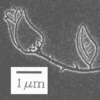
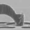
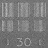
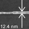
Sample Pictures - Also see the Diagnostic Images
-
User Notices - The NPGS v9.2 Upgrade which supports QCAD for pattern design is now available
For additional information, please contact:
 Joe Nabity, Ph.D.
JC Nabity Lithography Systems
P.O. Box 5354
Bozeman, MT 59717 USA
(406) 587-0848
info@jcnabity.com
www.jcnabity.com
New links or information added to the NPGS web site:
Direct write Pt patterning with NPGS using
EBID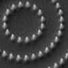
Template Stripped Nanostructures
NPGS: The highest performance / lowest cost direct write Lithography System for over 20 years!
The last update of this site was on February 21, 2025.
Copyright (c) 2025 JC Nabity Lithography Systems. All rights reserved.