|
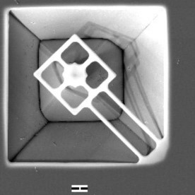
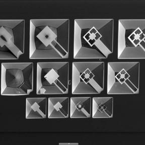
These two images display "Tunnel-tip" structures. The objective is to obtain
a 'pyramidal tip' of silicon that is pointing up and is very close to a metal
pad that covers it from top. Normally, the metal pad is used for etching
a tip below it and is 'sacrificed' when the tip actually gets formed (the
pad has no supports and hence falls off). The work shown here demonstrates
a technique where a pad has been designed in such a way that it allows tip
to be etched but does not fall off.
The image on the left shows a closeup view of a single device that has the tip just being formed below the pad. (The scale bar is 10 microns long.) Such a device can be used for measuring tunneling currents. The image to the right shows various cross-bridge patterns for metal pads. (The scale bar is 100 microns long.) The work is yet to be published. The work shown below was performed at the Tata Institute for Fundamental Research in Bombay, India. (These images were acquired with the NPGS Digital Imaging Feature.)
|
|
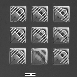
The image below displays autoranging torsion sensors that were conceived
as a result of a conscious effort to make the sensor 'do things by itself'.
This is a very important innovative concept in TRIZ - A Russian acronym for
Theory of Inventive Problem Solving. (The scale bar is 100 microns
long.) Results are still to be published.
|


