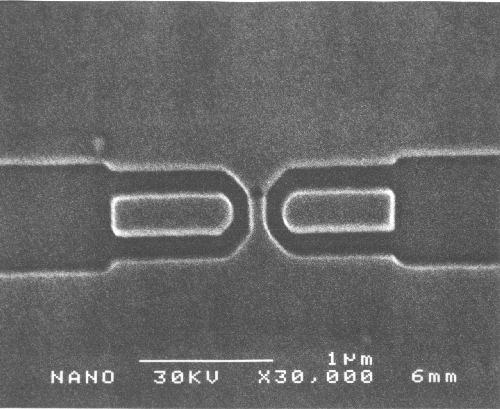
NPGS: Split Gate
 This
image shows a split gate structure. The gap shown is ~100 nm, while the smallest
gaps produced by the group has been 25 to 30 nm. The work was done at the
University of Sherbrooke in Canada. The next image
shows the bonding pads for this device.