NPGS:
Electron
Pump
Picture Menu | Main
Menu
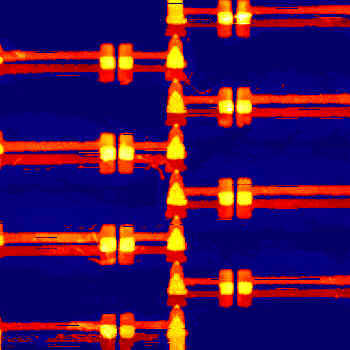 This
scanning force microscope image shows a 7-junction electron pump fabricated
at NIST in Boulder, CO. (The thin horizontal streaks are artifacts from the
scanning force microscope.) The pattern was written in a bilayer of PMMA
to create a mask with large undercut. A double-angle evaporation technique,
with oxidation after the first layer, was then used to create small tunnel
junctions where the two layers overlap. The seven small bright dots down
the center are the tunnel junctions (~40 nm x 40 nm) and the larger structures
along the sides are gate capacitors which allow control of tunneling of
individual electrons. The distance between junctions is 0.6 µm. This
device can pump individual electrons with an error of only 1 part in
108, and is the basis for a new type of capacitance standard.
See M.W. Keller et. al., Appl. Phys. Lett. 69, 1804 (1996).
This
scanning force microscope image shows a 7-junction electron pump fabricated
at NIST in Boulder, CO. (The thin horizontal streaks are artifacts from the
scanning force microscope.) The pattern was written in a bilayer of PMMA
to create a mask with large undercut. A double-angle evaporation technique,
with oxidation after the first layer, was then used to create small tunnel
junctions where the two layers overlap. The seven small bright dots down
the center are the tunnel junctions (~40 nm x 40 nm) and the larger structures
along the sides are gate capacitors which allow control of tunneling of
individual electrons. The distance between junctions is 0.6 µm. This
device can pump individual electrons with an error of only 1 part in
108, and is the basis for a new type of capacitance standard.
See M.W. Keller et. al., Appl. Phys. Lett. 69, 1804 (1996).