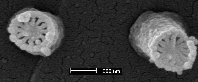
In this case, the beam had sat nearby since there was not a beam blanker on the SEM, and consequently, a ~10 micron diameter area was fully exposed (in the positive sense) in the PMMA, which is common when a blanker is not used. Subsequently, the wheel pattern was inadvertently exposed at an SEM magnification of ~30,000x, rather than the 1,000x that the run file had called for, which caused the wheels to be written within the 10 micron diameter exposed area. The result was that the pattern was written ~30 times smaller than the desired size, i.e., the wheels which were designed with a diameter of 10 microns were exposed with a diameter of about 300 nm. By chance, the total dose was such that the wheel structures crosslinked the PMMA to produce the structures shown. Note that the original resist was about 400 nm thick, which seems consistent with the apparent height of these structures.
Click to see another example of high resolution negative tone PMMA lithography.
The two important points to learn are:
1) If the SEM magnification is set to a value that is different from the value entered in NPGS, the pattern size and dose can be significantly different from what was intended.
2) When PMMA is given a very high dose, it will respond as a negative resist, and in this case, with 50 nm resolution or better. (The bumps on the structures appear to be grains from the metal coating, which are also seen directly on the substrate between the wheels.)
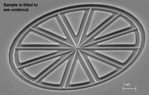
 This
images shows the wheel pattern written in PMMA at 4 kV. In this case,
the dose was high enough to crosslink the PMMA where the beam hit on the
wheel pattern (narrow spokes and rim) and the proximity effect at 4 kV exposed
the resist less than ~1/2 micron on either side of the exposed lines.
The undercut of the remaining PMMA is clearly seen due to the tilt of the sample when the image was taken.
It is interesting to note that the center area of cleared PMMA shows the proximity effect where the 12 spokes converge, however, the narrow lines of crosslinked PMMA do not show such a large effect.
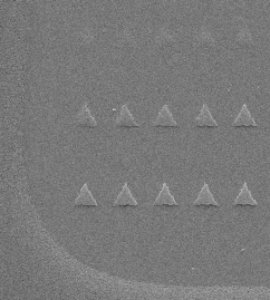
 This image shows an array of
triangles on a ~1 micron spacing, where the exposure was at a dose high enough
to turn the PMMA negative. (The sample was coated with metal for viewing
after a normal development for PMMA.) In this image, the first row of the
array can barely be seen, however, the higher doses are very well defined.
A closer image of high dose triangles are shown below. (The rough edges seen
in this image are an artifact of the pixel size of the image, not of the
pattern writing.)
Note the rounded border seen in the lower left part of the image. Near the triangles, the proximity dose has caused the PMMA to be fully developed away (as normally happens when PMMA is exposed with a typical dose level), while the border shows the edge where the PMMA was far enough from the exposed areas such that it was not developed away. This cleared area around the written structures and the curved edge of the border around the pattern indicates that the dose of the pattern was very high. As in the case of the wheels above, this exposure was caused when the magnification of the SEM was left at a value much higher than the run file indicated.
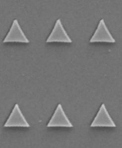
 This image shows triangles that
were exposed at a dose high enough to make PMMA respond as a negative resist.
The side length of the triangles is about 1/2 micron.
Note that while the area between these triangles is cleared of any PMMA, the image above shows that away from the exposed areas, the PMMA will not be developed, since it will be far enough away so that it does not get a significant proximity dose.