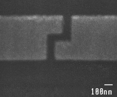
NPGS: Double Bend Point Contact

This picture shows a double bend in a split-gate field-effect transistor. The substrate consists of MBE grown AlGaAs on undoped GaAs. Even though the width of the gap is only 100 nm, notice how the corners are quite sharp. - Pattern written by Dr. J.C. Wu while at University of Oregon. He is now at National Chang-Hua University, Taiwan.