NPGS: Detailed Structures
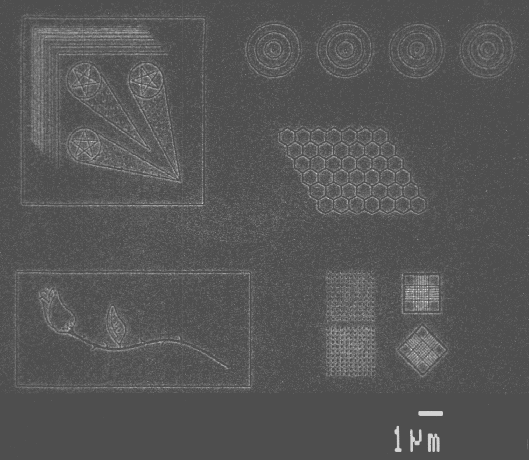 These structures were written in a single layer of PMMA using a
5 pA beam at 40 kV. The finest linewidths are ~30 nm. The SEM picture
was taken after the sample was developed and coated with gold for
viewing. The roughness in the picture is an artifact of the scanning
process used to digitize the image. See the Rose,
Hex Grid, and 45 Degree Box
images for clearer views at higher magnifications.
These structures were written in a single layer of PMMA using a
5 pA beam at 40 kV. The finest linewidths are ~30 nm. The SEM picture
was taken after the sample was developed and coated with gold for
viewing. The roughness in the picture is an artifact of the scanning
process used to digitize the image. See the Rose,
Hex Grid, and 45 Degree Box
images for clearer views at higher magnifications.