 The
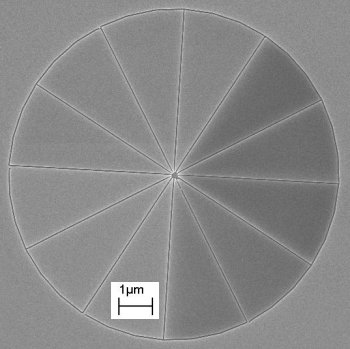
first two images show what charging can look like in lithography patterns
when the developed resist is viewed in an SEM after being coated with metal.
In this case, the surface of each wedge of resist is completely surrounded
by written lines. If the lines have good undercutting, the metal on
the top of each wedge of resist can be completely isolated from the rest
of the metal used to coat the sample. The isolated areas can then charge
when viewed in the SEM and appear darker than the surrounding metal.
Sometimes the charging area will appear nearly completely black.
As is shown here, only some of the wedge structures will charge, since others will have enough of an electrical connection to discharge. In general, sputter coated samples are less likely to display this effect, however, this particular sample was sputter coated, which indicates it had very good undercutting. These linewidths are ~80 nm and the resist is ~200 nm thick.
The periodic "ripples" in the lines at 3, 6, 9, and 12 o'clock are an imaging artifact that appear when the pixel size of the image is approximately the same as the linewidths.
Also see the general SEM Optimization Guide and the SEM Lithography Setup Guide.
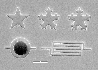
 In this image, the
pattern consists of five filled polygons, where the circular structure has
an "island" of unexposed resist in the center which is charging even though
the sample has been coated with metal. (The scale bar is 10 microns long.)
Such charging is more common when the resist is coated using a directional source such as an evaporation system, while sputtered metal is more likely to coat the edges and prevent the charging. Similarly, evaporated metal is more likely to produce a clean lift-off, while sputtered metal is more likely to produce a poor lift-off. While charging can produce unusual looking images, the charging is a good sign, since it indicates a good undercut in the resist side wall.
Note that this pattern is also slightly underexposed, as can be seen by the few remnants of resist (bright spots) in the bottom of the exposed part of the circular structure. Also, the serpentine structure in the lower right displays a common bright/dark edge artifact seen when straight lines are almost parallel to the scan axis in a digitized image. The same effect is seen more dramatically in the middle picture on the USA map page.
A non-charging view of the pattern shown above can be seen here. Note that this other image is fully exposed and the higher resolution of the digitized image eliminates the artifacts on the serpentine structure.
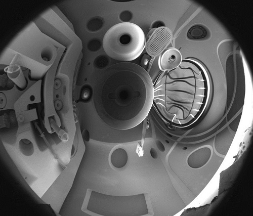
 This
image is not directly related to lithography, but is still quite interesting.
The image shows an inside view of the top of the chamber where
the dark circular structure in the center is the final lens of the SEM column.
When imaging an insulating feature, it is possible for enough charge to accumulate that the feature can act as a spherical mirror with respect to the incoming beam of electrons. This image was acquired at 500 eV at a WD of ~10 mm after an area on a flat piece of sapphire was charged by the e-beam.