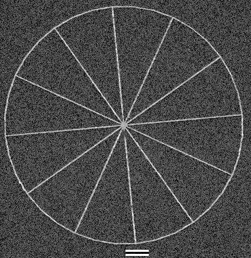
 This
image displays the "wheel" pattern with ~50 nm metal lines after a nearly
perfect liftoff. The marker at the bottom is 1 micron long. The pattern was
written by Alex Kozhevnikov at Yale University. (This image was acquired
with the NPGS Digital Imaging Feature.)
Note that for lines of this size and smaller, the grain size and continuity of the deposited metal significantly affect the quality of the resulting structure. Also, rough edges can result if the metal film coats the sidewalls of the resist and then rips during liftoff. These effects are shown in the images below.
Also see the general SEM Optimization Guide and the SEM Lithography Setup Guide.
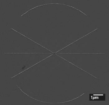
 This
image shows a "wheel" pattern after liftoff that was written with astigmatism
in the beam. The lines are ~30 nm wide and consist of ~20 nm thick Ti on
Si.
In this case, when the pattern was written, the beam had astigmatism such that it was elongated in the horizontal direction. Lines written in the long direction of the beam received all of the dose in a narrow line, while in the perpendicular direction, the beam was effectively spread over a wider area, thus resulting in underexposed lines.
When first learning to do lithography, lift-off should ONLY be attempted AFTER the coated samples have been viewed in the SEM. The reason is that even poorly exposed patterns can be viewed after coating and they can give useful information on the optimization of the SEM during the pattern writing. However, if liftoff is performed on a poorly exposed sample, little, if any, of the structures will remain, which leaves no useful information as to what aspect of the writing needs to be improved.
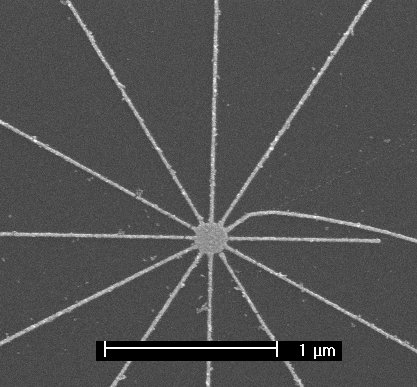
 This
is an image of the "wheel" pattern after a less than perfect liftoff. (To
see a wheel pattern from the same sample before liftoff, click
Wheel #1.)
The liftoff was done by letting the sample soak in acetone (at room temperature) for about 10 minutes, followed by rinses in acetone, IPA, and DI.
The linewidths are ~30 nm and the metal is ~30 nm thick gold that was evaporated onto a silicon substrate. The resist was ~200 nm thick.
The grain size of the gold is ~ 10 nm, which is why the edges of the lines look so rough. Also, it is apparent that the gold does not stick well to silicon. In general, pure gold is not a good choice for a silicon substrate when lift-off is to be performed.
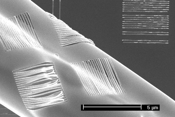
 This
interesting image shows an unsuccessful liftoff attempt where the metal film
has only partially peeled away from the substrate (dark area). The bright
edges on the lines that did adhere to the substrate indicate that the
resist did not have sufficient undercutting to prevent the metal from coating
the edges of the developed areas in the resist. Consequently, during lift-off
the metal on the edges sometimes ripped and left bright "flags" of metal
on the edges of the lines on the substrate and when the metal did not rip,
the line was peeled off of the substrate.
Note that the set of lines shown in the peeled back metal that is directly above the scale bar can be matched to the horizontal lines on the substrate, since careful inspection reveals that the missing lines from the substrate are still attached to the metal film.