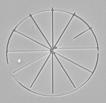
 These
images show distortions which were caused by localized charging of the substrate
as the pattern was being written. See below for solutions to this
type of problem using conductive layers or a
VP SEM.
Note that the resist itself will typically charge even when using a conductive substrate, however, the resist will usually be thin enough that the accumulated charge is not enough to degrade the writing. In this case, the substrate was a bulk insulator, and the charging effects were quite significant. Any insulating layer that is thicker than the penetration depth of the incident electron beam will act as a bulk insulating substrate.
In this image, the "spokes" of the "wheel" were written in a counter-clockwise sequence starting with the line in the 3 o'clock position. As the image was written, the localized charging shifted the beam such that the wedge of resist defined by the first spoke (at 3 o'clock) and last spoke (at 4 o'clock) ended up significantly larger than the others. The outer circle was written after the spokes and has also been shifted such that it does not line up properly.
Also, astigmatism can be seen as evidenced by the fully exposed lines in the vertical direction and the under exposed lines in the horizontal direction.
Note that the defect in the 2 o'clock spoke and in the circle at ~8 o'clock were caused by a intermittent noise that has been seen in the SEM used for the writing.
Also see the general SEM Optimization Guide and the SEM Lithography Setup Guide.
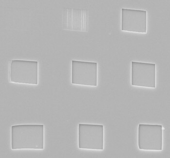
 This
image shows an array of 10 micron square boxes that was written on
the same GaN substrate as above, which was only somewhat conductive.
(All images were taken after development and sputtering with Au.)
Note that the dose for each box was varied to determine the ideal exposure, where the upper left box (virtually invisible in this image) has the lowest dose and the lower right box has the highest dose.
The identical pattern is seen below after being written on a different GaN substrate which was more conductive.
 This
is the identical pattern as seen above, however, it was written on a different
GaN substrate which was more conductive than the one in the upper images.
Using conductive coatings to solve the problem:
The typical solution is to to add a conductive layer either above or below the resist. The choice of conductor (metal, polymer, etc.) will depend on the details of the application. In some cases, it may be difficult to determine a coating/removal process that is compatible with the entire device fabrication process.
One simple solution to prevent pattern distortion from charging is to evaporate ~10 nm of aluminum on top of the resist before writing and etch it off in NaOH or KOH after the writing and before developing. The etch recipe is to use several pellets of NaOH in ~100 ml of DI water and etch for about 30 seconds. (You can coat some test samples and try various concentrations and times to optimize the process, if necessary.) Note that NaOH may permeate the PMMA and chemically interact with some substrates.
Another recipe for etching aluminum is to use a very weak HF solution (50% by weight diluted 100:1) for a few seconds, followed by a DI water and then IPA rinse.
Also, "ESpacer" (PDF product sheet) is a commercial charge dissipating agent (based on a conductive polymer) which is made by Showa Denka for use in e-beam lithography. Another option is "aquaSAVE" from Mitsubishi.
Using a Variable Pressure SEM to solve the problem:
A new technique to reduce the effects of localized charging during lithography is described in the paper:
Variable Pressure Electron Beam Lithography (VP-eBL): A New Tool for Direct Patterning of Nanometer-Scale Features on Substrates with Low Electrical Conductivity
Myers, B. D.; Dravid, V. P.,
Nano Lett.; (Letter); 2006; 6(5); 963-968.
This paper describes using NPGS and the standard variable pressure feature of a VP capable field emission microscope to reduce the charging during the writing. The paper states that on electrically insulating substrates, the authors "are able to achieve line widths comparable to those achieved with high vacuum exposure on conductive substrates (<20 nm)."