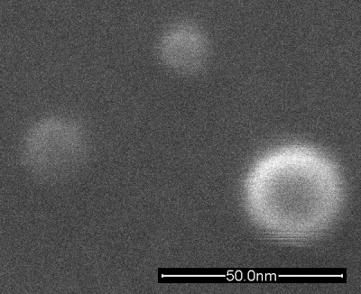
 This
image shows three "Contamination Spots" that were made before writing patterns.
This
image shows three "Contamination Spots" that were made before writing patterns.
These spots are extremely useful during lithography, because they can be used to confirm that the beam is well astigmated and well focused immediately before writing patterns. They can also be used after writing patterns to check if the beam quality has changed during the writing.
In general, when using a thermal FE SEM, if contamination spots can be made that are 30 nm or less, the best lithography in 950k PMMA will typically be of a similar or smaller size.
Contamination spots can be made directly on the surface of the resist by leaving the focused beam stationary for ~1 to 30 seconds, either by setting the microscope to "Spot" mode or to external control while NPGS has the DAC voltages set to (0,0).
In this case, the bright (~30 nm) diameter spot was made in about 10 seconds, while the small (~10 nm) spot was made in about 1 second. Note that the spots will continue to grow in size during imaging, and these spots were somewhat smaller and better defined before the image was aquired.